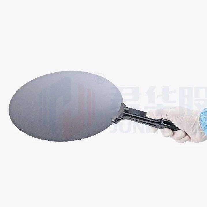
In the global integrated circuit manufacturing sector, capacity constraints have become the norm, driving significant investment in integrated circuit-related fields in China over the past two years. This investment boom has not only fueled the rapid development of the semiconductor device equipment, electronic components, and specialized electronic materials manufacturing industries but also spurred a surge in demand for high-performance materials like PEEK.
PEEK (polyetheretherketone) material, with its exceptional high-temperature resistance, wear resistance, dimensional stability, chemical corrosion resistance, and ease of processing, has demonstrated unparalleled advantages in semiconductor manufacturing. Particularly in the field of wafer clamping, PEEK wafer clamps have become an indispensable tool due to their unique properties. These clamps ensure wafer integrity, significantly enhance production efficiency, and improve yield rates. Consequently, PEEK wafer clamps are gaining increasing attention and widespread application in the semiconductor industry.

The core advantages of PEEK wafer clamps are as follows:
1. Contamination-Free Clamping
PEEK wafer clamps use modified PEEK granules with extremely high purity, containing virtually no trace elements that could contaminate silicon wafers. This ensures absolute safety during the clamping process.
2. Anti-Static Protection
PEEK wafer clamps possess excellent anti-static properties, with surface resistivity ranging from to Ω. The resistivity of the clamp heads can even reach -Ω, effectively preventing electrostatic discharge (ESD) damage to silicon wafers and providing comprehensive protection.
3. High-Temperature Stability
PEEK wafer clamps can operate in high-temperature environments of up to 260°C while maintaining high strength, dimensional stability, and a low coefficient of thermal expansion. Their superior resistance to sliding and fretting wear ensures no scratches or residues on the surface of wafers or silicon chips during clamping, thereby preserving surface cleanliness.

Notably, the PEEK5600ESDZ01 granules developed by Junhua Co. represent an anti-static material designed specifically to address static electricity issues. With a stable and controllable surface resistivity ranging from to Ω, this material exhibits exceptional performance in anti-static properties, processability, and appearance. It finds extensive application in electronics, semiconductors, and the petroleum industry, effectively reducing losses caused by static electricity.
Additionally, these anti-static granules are used in explosion-proof product casings and structural components, such as electrical product casings and structural parts in coal mines, oil tankers, and oilfields. This demonstrates their broad application prospects and enormous market potential.