
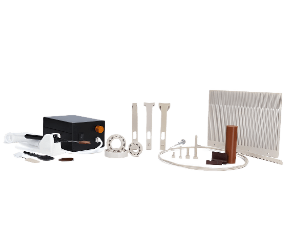
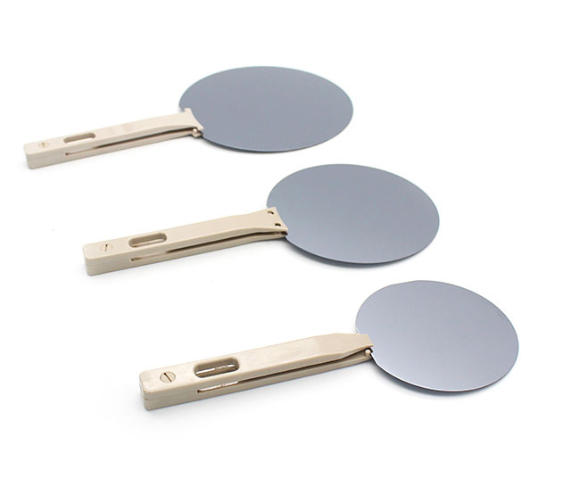
PEEK wafer clamps
PEEK has many advantages in the field of electrical semiconductors:
- • Very high temperature resistance (up to 260°C continuous operating temperature)
- • Excellent chemical resistance
- • Good dimensional resistance (low thermal expansion)
- • Optimal ratio of stiffness, solidity, toughness and minimal tendency to creep
- • Very good tribological properties
- • Good radiation resistance
- • Excellent resistance to hydrolysis
- • Fire performance: flame-retardant, Low smoke density, No toxic gases
- • Good machinability
- • Good bondability and weldability
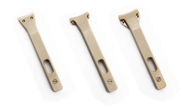
Typical product: PEEK chip clip, PEEK vacuum sucket, CMP ring, PEEK vaccum tweezer, PEEK screw
PEEK solutions in the electronics industry
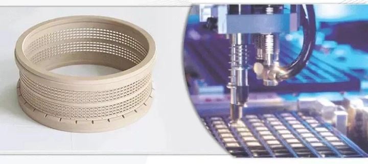
A very important step in silicon wafer production is the Chemical Mechanical Planarization (CMP) process. The trend is towards larger wafer sizes, smaller chips with narrower line widths and feature sizes. The challenge is to find a material with the desired characteristics, as the CMP process requires components made of highly qualified materials. In close cooperation with customers, we have specialised in developing materials that meet these requirements.
For continuous plating of point-to-point terminals, the thickness and height of the plated layer can be precisely controlled by the PEEK selector ring, resulting in significant savings in gold loss.
PEEK is widely used on consumer electronics, home appliances and semiconductor products for electronic industry. PEEK polymers can withstand continuous use high temperatures and harsh chemicals, modified peek provide a range of electrically conductive, anti-static or static dissipative properties, these characteristics are important for semi-conductor applications such as vacuum traceless sucker.
JUNDE PEEK solution to suit every environment and meets the strictest requirements, based components have a proven cost less than traditional materials, such as replacing metal with integrated PEEK components can improve energy efficiency in appliances up to 2% by weight reduction, help increase fab productivity up to 3% with longer lifetime than PPS.
Team up with JUNDE PEEK to address your challenges in the ever-changing electronics industry.
Explore our PEEK-type Solutions
PEEK has many advantages in the field of electrical semiconductors:
Very high temperature resistance (up to 260°C continuous operating temperature)
Excellent chemical resistance
Good dimensional resistance (low thermal expansion)
Optimal ratio of stiffness, solidity, toughness and minimal tendency to creep
Very good tribological properties
Good radiation resistance
Excellent resistance to hydrolysis
Fire performance: flame-retardant, Low smoke density, No toxic gases
Good machinability
Good bondability and weldability
Typical product: PEEK chip clip, PEEK vacuum sucket, CMP ring, PEEK vaccum tweezer, PEEK screw
We will be in very short time to give you a satisfactory answer.
CASE STUDY – CMP Ring
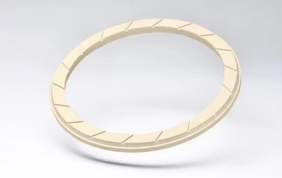
A very important step in silicon wafer production is the Chemical Mechanical Planarization (CMP) process. The trend is towards larger wafer sizes, smaller chips with narrower line widths and feature sizes. The challenge is to find a material with the desired characteristics, as the CMP process requires components made of highly qualified materials. In close cooperation with customers, we have specialised in developing materials that meet these requirements.
Product Processing and Quality Control Capability
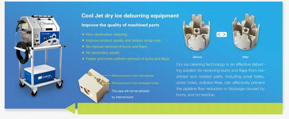
Cool Jet dry ice deburring equipment
Improve the quality of machined parts
Non-destructive cleaning;
Improve product quality and reduce scrap rate;
No manual removal of burrs and flaps;
No secondary waste;
Faster and more uniform removal of burrs and flaps.
Dry ice cleaning technology is an effective deburring solution for removing burrs and flaps from machined and molded parts. Including small holes, cross holes, pollution-free, can effectively prevent the pipeline flow reduction or blockage caused by burrs, and no residue.
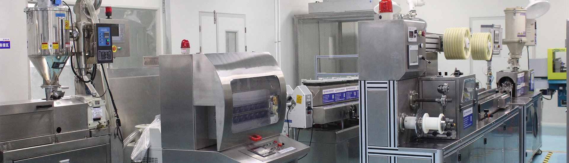
100,000-level cleaning workshop
Our company has established a 280-square-meter, 100,000-level cleaning workshop and equipped with 100-level cleaning area in accordance with GMP requirements.